HOLOGRAM, IT’S HISTORY,
MANUFACTURING AND APPLICATIONS
Dr. Wiriyah Chupaween, Ph. D.
President
Azure Photonics Co., Ltd.
INTRODUCTION
Holograms have been introduced into Thailand since the late 80s. Nowadays we could say without exaggeration that in Thailand we can find plenty of occasions seeing examples of hologram applications.
Purposes of the applications are diversified. For examples, security or authentication for documents and ID cards, anti-counterfeiting and brand protection for commercial items, decoration of packaging, coupons for sale promotion, new artistic features for printing materials, etc. Two most important applications of holograms, however, are for security and packaging.
Thailand’s hologram market used to totally rely on imports from North America, Europe, Taiwan, and China. With the founding of Azure Photonics Co., Ltd., in 1999, hologram manufacturing industry had been established in Thailand, supplying the domestic hologram market and exporting to a number of countries.
BRIEF HISTORY
The birth of holographic technology took place in 1948 when Noble Prize laureate D. Gabor invented hologram [1] as a means for recording and replaying image in the form of light waves. The optical quality of those days’ holograms, however, was limited due to the lack of a genuine coherent light source. Therefore, with the coherent light waves available from the laser that was invented in 1959, E. N. Leith and J. Upatnieks further revised the hologram technique and spectacularly improved the optical quality of holographic images in 1962[2].
Since then a great number of techniques and materials had been proposed to exploit the tremendous potential of the hologram as a new media for recording, storage and replay of information and images. Among them were rainbow holograms proposed by S. A. Benton (1969) [3], and dot matrix “holograms” by different persons and companies (1980s – 1990s). Along with the evolution of holography, different technologies for mass production of holograms were also explored and developed.
Hologram embossing has been the most popular manufacturing technology. Developed in the late 70s, this technology is for manufacturing very high quality hologram replicas at very high speeds. In such a production process, the surface-relieved information on a rainbow hologram and/or dot matrix “hologram” (see explanation in the text to follow) is being transferred to replicas. The first significant commercial application of embossed holograms probably was the small 3D image hot-stamped on Visa cards in 1982. If the scale of the project and the impacts it brought about could be considered the start of an industry, then the embossed hologram manufacturing industry is now 30 years of age.
It might be worthwhile to mention Thailand’s first pilot factory for embossed hologram manufacturing that the author established and started operating in 1994 for NECTEC (The National Electronics and Computer Technology Center), on the campus of King Mongkut Institute Lardkrabang. The governmental program introduced, for the first time, hologram embossing technology into Thailand as part of the efforts for promoting photonics industries in the country. The achievement of the program was recognized internationally and in 1997 was among the sixteen hologram manufacturing countries listed in an authoritative sourcebook of the worldwide holographic industry, “Holography Market Place, the hologram industry reference text and sourcebook”[4].
BASIC HOLOGRAPHY
A unique media storing an image for replay, the hologram is totally different from other kinds of image media, such as photos, paintings, drawings, movies, and video/computer monitors, etc. The fundamental characteristics of the hologram lie in the fact that its image is handled in the form of light waves. In other words, the hologram does not store the image explicitly. Instead, what the hologram stores is a physical record of the light waves that came out from the imaging object. Using this record one can replay the light waves to optically realize the stored image. In practice, all what is needed to visualize a hologram image is just a beam of light. More accurately speaking, when illuminating a hologram with a beam of light in a particular manner prescribed for the hologram itself, the image will be replayed with all its colors and shapes in a 3D manner. No inks and color filters are involved in the recording and replay processes. And for embossed holograms, the embossing process of the hologram image on the plastic film takes only one single operation: all colors are recorded (“printed”) simultaneously onto the hologram replica in one single embossing operation (“printing”).
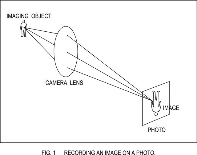
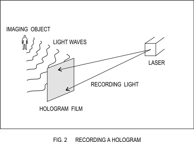
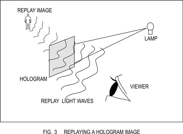
Figures 1 and 2 illustrate the difference between a photo and a hologram in terms of image recording. When doing recording of a hologram, one needs a recording laser beam to join with the image light wave at the surface of the hologram recording film. What the hologram film records is a set of extremely fine patterns, the resolution of which is equivalent to 50000 DPI to 150000 DPI. These fine patterns are the interference fringes mutually formed by the image light wave and the laser light wave. Comparatively, replaying the hologram image is much easier. As seen in Figure 3, the replay light source can be just an ordinary light bulb. When the replay light beam illuminates the hologram in a manner similar to the setting of the recording laser beam, the stored image will be visualized. The size and the color spectrum of the replay light, however, will influent the optical quality of the image, depending on the particular type of hologram one has made.
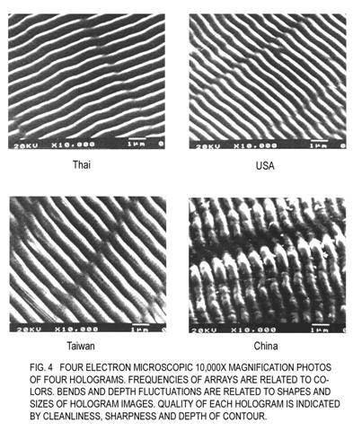
A hologram in nature is a record of the interference fringes from which the image wave can be retrieved in the replay step. The record is made on a layer of high resolution, light sensitive material, around one to ten microns thick. The fine interference fringes spread to the whole area where the two beams meet. When the recording layer is placed within the interference field, the distribution of the light intensity will penetrate into the layer and then get recorded. The volume of the recorded information about the intensity distribution is therefore proportional to the area and thickness of the recording layer. In the hologram manufacturing industry, the original hologram is of surface-relieved type. The recorded information takes the form of fine grooves on the surface, at most half a micron deep. Therefore, the viewable depth of a 3D image observed from an embossed hologram usually is only about a few mm. Fig. 4 shows four 10000x magnified electron microscopic images of the surface structures of four embossed holograms made in Thailand and other three countries.
Similar to the genuine hologram, dot matrix “holograms” display dazzling colors when being illuminated. However a dot matrix “hologram” in nature is just a pile of many tiny dots, each of them being a diffraction gratings. By distributing the dots in certain patterns and arranging the light diffraction angle of each of the dots in certain manners, various dazzling visual effects can be achieved. The structure of the gratings is as fine as that of the genuine hologram, but the distribution density of the dot matrix usually is around several hundred DPI, though 3000 DPI or more could be achieved. The gratings of the dots are also of surface-relieved type. They can be reproduced by means of surface embossing. This explains why dot matrix “holograms” are available as products of the hologram industry.
In comparison, a genuine hologram is more suitable for replaying 3D images, while a dot matrix “hologram” is more convenient for creating visual effects. Combining both types on a single hologram therefore allows more freedom of creation.
MANUFACTURING PROCESS
In principles, all kinds of holograms can be copied or replicated, either by means of light exposure or embossing or else. In the case of embossing, the master hologram must be of surface-relieved type, i.e., the hologram information is stored on the surface in the form of fine grooves (see Fig. 4). An embossing stamper can be made by replicating the master hologram (on the surface of a photoresist layer) by means of electroforming. Then in the embossing process the hologram information is being easily transferred from the stamper to the surface of a thin film of plastics such as PET, BOPP, PVC, etc. Such a manufacturing process can be illustrated using the flowchart in Fig. 5 as follows:
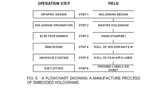
FIG. 5 A FLOWCHART SHOWING A MANUFACTURE PROCESS OF EMBOSSED HOLOGRAMS.
Details of actual operation in the industry environment might vary from time to time in order to meet the customer’s particular needs. Necessary adjustments could be made at any operation step, which might involve operation parameters, materials used, and equipment alteration. Furthermore, continued innovation is the most powerful weapon for Thai hologram industry to remain competitive in both domestic and international markets.
PRODUCTS AND APPLICATION TRENDS
Products of the hologram industry are increasingly diversified. In general they fall into three basic categories: hologram film, hologram foil and hologram paper. These categories can be further categorized as transparent or metallized, types of adhesive coats, etc. For different applications finished hologram products may take diversified shapes and forms.
The last two decades had witnessed continuous growths of the hologram industry despite fluctuations in the global economic environments. Continued expansion of hologram applications in security and packaging are the true propelling forces.
REFERENCES
- D. Gabor, “A New Microscope Principle,” Nature 161, 777 (1948).
- E.N. Leith and J. Upatnieks, “Reconstructed Wavefronts and Communication Theory,” J. Opt. Soc. Amer. 53, 1123 (1962).
- S.A. Benton, “Hologram Reconstruction with Extended Light Sources,” J. Opt. Soc. Amer. 59, 1545 (1969).
- Holography Market Place, 6th Ed., ed. by F. Ross and A. Rhody, pp. 174-5 (1997).


